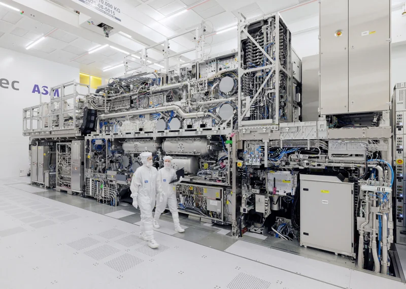
At the heart of modern semiconductor manufacturing, a machine that appears unassuming is quietly redrawing the boundaries of human technology. It’s the extreme ultraviolet (EUV) lithography machine. This technology etches billions of transistors onto silicon wafers with nanometer-level precision, forming the foundation for smartphones, AI chips, and supercomputers. As one engineer put it: “The precision of an EUV lithography machine is influenced by the Moon’s gravity—and that’s no exaggeration.” Why would a machine on Earth be affected by a “distant greeting” from 384,000 kilometers away? In this article, we’ll dive into the principles of EUV lithography, its precision mechanisms, and how it counters cosmic-scale interference, revealing the pinnacle of human engineering ingenuity.
The Core of EUV Lithography Machines: Crafting a Nanometer-Scale “Brush”
To grasp the precision of EUV lithography, we first need to revisit its working principles. Traditional lithography machines use visible light or deep ultraviolet (DUV) light with wavelengths around 193 nanometers, which struggles to meet the demands of chip nodes below 7 nanometers. EUV lithography revolutionizes this by employing extreme ultraviolet light at just 13.5 nanometers—a wavelength that’s nearly “invisible” in the electromagnetic spectrum, over 10 times shorter than visible light. Why such a short wavelength? Chip features have shrunk to mere nanometers (the width of just a few dozen atoms), requiring the etching of billions of transistors on a 300-millimeter-diameter silicon wafer. Shorter wavelengths deliver higher resolution, much like using a finer pen tip to draw more intricate patterns.
However, EUV light doesn’t exist naturally in Earth’s atmosphere—it’s strongly absorbed by air and ordinary glass, preventing transmission. So, engineers devised an artificial “light factory”: the light source generator, the beating heart of every EUV lithography machine. Leading the charge is Dutch company ASML, whose systems fire ultra-pure tin (Sn) droplets, just tens of micrometers in diameter, at speeds of 100 meters per second. A high-energy laser first strikes the tin droplet, flattening it into a pancake; then, a main pulse laser (packing up to 25,000 watts—10 times the power of lasers used to cut steel) instantly vaporizes it, creating a superheated plasma at tens of thousands of degrees Celsius, like a miniature sun. The entire machine operates in a high-vacuum environment at around 10⁻⁷ Pa to prevent the 13.5 nm EUV light from being absorbed.
Within this plasma, electrons drop from high-energy states and emit precise 13.5-nanometer EUV photons. The whole process must be controlled with millisecond precision and repeated 50,000 times per second for stable output. The optical path is equally demanding: since EUV light is so easily absorbed, the system can’t use conventional lenses and relies instead on multilayer mirrors to guide the beam. These mirrors, crafted by German optics giant ZEISS, have surface flatness deviations controlled to within nanometers. If you scaled up one of these mirrors to the size of Germany, its tallest bump wouldn’t exceed 1 centimeter. A single mirror reflects only 70% of the light; after bouncing through over 10 mirrors, just 10% reaches the wafer. This “light loss” is a steep price, but it unlocks unparalleled pattern accuracy.
Nanometer-Scale Synchronization: A “Hair’s-Breadth Brush” on a High-Speed Train
The core of EUV lithography is the exposure step: EUV light passes through the circuit pattern on a reticle (mask) and projects onto a photoresist-coated silicon wafer. The reticle and wafer stage must move in perfect sync—the wafer stage scans at speeds of several meters per minute, with errors under 1 nanometer. It’s like painting with a hair-thin brush from one speeding train onto another running parallel. Any tiny jitter could misalign the pattern and ruin the entire wafer.
Inside the EUV lithography machine, the synchronization between the wafer stage and reticle stage is hailed as “the most precise waltz in mechanical engineering history.” This isn’t just about matching speeds; it’s about real-time alignment across all six spatial dimensions:
1. Velocity Synchronization: A 4:1 “Chase”
The machine’s optical projection system typically features a 4:1 reduction ratio, meaning patterns on the reticle are four times larger than those etched on the wafer.
- Speed Ratio: To avoid stretching or blurring during scanning, the reticle stage must move exactly four times faster than the wafer stage.
- Instantaneous Acceleration: As the wafer stage hurtles forward at about 5g, the reticle stage endures a staggering 20g—several times the G-forces fighter pilots endure—reciprocating in milliseconds to reach steady speed.
2. Laser Interferometry: The Nanometer “Eyes”
To keep these high-speed “trains” on track, the system uses vacuum-based laser interferometry in a closed-loop control:
- Real-Time Monitoring: Laser beams fire at tens of thousands of times per second toward mirrors on the stages, measuring displacements with 0.1-nanometer accuracy—about the size of a single atom.
- Dynamic Correction: If the reticle deviates by even an atom’s width, control algorithms drive linear motors to compensate in microseconds, keeping the two stages in absolute relative stillness.
3. Magnetic Levitation Drive: Banishing Friction
At nanometer scales, any physical contact causes deadly friction and vibration.
- Full Suspension: The wafer and reticle stages don’t run on tracks; they’re propelled by planar motors, hovering frictionlessly in magnetic fields.
- Contactless Control: This eliminates mechanical wear and lubricant contamination, while enabling ultra-smooth adjustments in all six degrees of freedom (forward/back, left/right, up/down, and three rotations) to counter external disturbances, including crustal deformations.
4. The Art of Scanning: Seamless “Stitching”
Lithography isn’t a one-shot full-field exposure; it’s like a scanner using a narrow EUV slit to sweep across the surface.
- Coordinated Motion: As the reticle sweeps left to right through the beam, the wafer stage moves right to left in sync.
- Overlay Precision: A single chip requires dozens of such layers, with alignment errors (overlay) held under 1.5 nanometers. The wafer stage must maintain this sync through endless accelerations and decelerations over a full day’s run.
This precision is no fantasy: a stage weighing hundreds of kilograms can reposition itself in picoseconds (a trillionth of a second). It draws from over 5,000 global suppliers—U.S. lasers, German optics, Japanese ultrapure materials, Dutch assembly. No single nation could build it alone; it’s the crystallization of human industrial collaboration.
The Moon’s “Invisible Interference”: From Centimeters to Nanometers in a Chain Reaction
Why does such a precise system fall under the Moon’s gravitational sway? The answer lies in tidal effects. The Moon’s (and Sun’s) gravity, though faint, causes periodic deformations in Earth—tidal bulges up to tens of centimeters. These seem macroscopic, but they propagate as ground microseisms (centimeter-scale shifts) to the lithography stage, disrupting nanometer positioning. This force not only warps the crust (solid tides) but also alters local microgravity and groundwater pressure, subtly deflecting precision optics.
Specifically, lunar tides make Earth’s surface “breathe” twice daily, with amplitudes from millimeters to centimeters. For EUV lithography, this is like an earthquake: a 1-nanometer stage shift could skew transistor patterns and slash chip yields. Studies show that even in cleanrooms, tidal effects introduce 0.1–1 nanometer errors. It’s not science fiction—ASML engineers model lunar orbits from the design phase to predict and mitigate these disruptions.
More broadly, EUV machines face earthquakes, temperature fluctuations, and human-induced vibrations. At nanometer scales, any perturbation amplifies like a butterfly effect.
Engineering Ingenuity: Nanometer Compensation in “Breath Sync”
Faced with cosmic interference, engineers don’t surrender—they deploy multilayer defenses. First, active pneumatic isolation: the machine floats on air cushions, blocking ground vibrations from 1 Hz to 1,000 Hz, including low-frequency tidal quakes. It’s like an “airborne island,” decoupling the device from Earth.
Second, built-in high-precision sensors (like laser interferometers) monitor all six degrees of freedom in real time. Paired with advanced algorithms, the system compensates in nanoseconds—when Earth “breathes,” the stage subtly adjusts to keep the reticle and wafer aligned. ASML’s TWINSCAN EUV series even holds total overlay errors under 1.5 nanometers.
These aren’t standalone feats: global collaboration ensures seamless integration from materials to software. The payoff? A $200 million machine that produces chips powering the AI revolution.
Epilogue: Humanity’s “Lunar Waltz” in Technology
Today’s EUV tech—especially High-NA (high numerical aperture) variants—is the sole path for companies like NVIDIA to fabricate next-gen AI chips, underscoring how this precision game sets the ceiling for human computational power. The EUV lithography machine isn’t just the crown jewel of semiconductors; it’s humanity’s ultimate quest for precision. Born from laser-“blasted” tin plasma, it captures light and shadow on nanometer mirrors, steadying its course amid the Moon’s gravitational “dance.” That line—”not an exaggeration at all”—captures its wonder: when we gaze at a chip, aren’t we also peering at the stars? As physicist Richard Feynman said, “Nature isn’t trying to trick us; it’s inviting us to go deeper.” Under EUV’s glow, humanity is scripting its own cosmic chapter.
Further Reading:The Ice “Superpower” Awakens: Flexoelectricity in Ice Unlocks New Clues to the Origin of Lightning


